Leading expert in copper chip wiring technologies, Edelstein served as Chief Architect and driving force behind IBM's copper chip wiring technologies, first announced in 1997. These were devised to increase the speed and reliability of modern integrated circuit chips while enabling their further miniaturization. These wires, about 1/1000 the size of a human hair, carry signals among the transistors on a silicon chip.
Named an IBM Fellow in 2006 — the company's most prestigious technical honor — Edelstein has served as Manager of BEOL Technology Strategy at the Thomas J. Watson Research Center, Yorktown Heights, NY. His work has focused on CMOS on-chip Cu-based interconnection technologies, including low-k dielectrics, reliability physics, performance modeling and measurement, and evaluation of new materials and integration schemes.
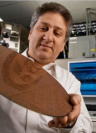
More recently, he led IBM's change from glass to a novel low-dielectric insulator between the copper wires, for a further speed increase. A modern microprocessor, itself about the size of a thumbnail, contains over a mile of copper wiring. IBM implemented this wiring in all its semiconductor products, including those that power its information technology systems.
The global semiconductor industry reoriented to follow the copper wiring architecture and roadmap which Edelstein defined. He is recognized as the leading expert in this field. On May 24, 2006, he was one of eight honorees named IBM Fellow.
From 1990 to 2008, he authored or co-authored several publications, just a few of which are: In 2007, "Non-Poisoning Dual Damascene Patterning Scheme for Low-k and Ultra Low-k BEOL," with W. Cote, C. Bunke, P. Biolsi, W. Wille, H. Baks, R. Conti, T. Dalton, T. Houghton, and W. Li, Advanced Metallization Conference 2006 (AMC 2006), 2007; and "Optimization of silicon technology for the IBM System z9," with T. Ivers, S. Narasimha, T. B. Faure, J. H. Rankin, D. A. Grosch, M. D. Knox, M. Khare, G. B. Bronner, H. J. Nam, and others, IBM Journal of Research and Development 51(1–2), 5–18, Citeseer, 2007.
In 2008, "Interface engineering for high interfacial strength between SiCOH and porous SiCOH interconnect dielectrics and diffusion caps," with A. Grill, M. Lane, V. Patel, S. Gates, D. Restaino, and S. Molis, Journal of Applied Physics 103, 054104, 2008; and "Performance and reliability of airgaps for advanced BEOL interconnects," with S. Nitta, S. Ponoth, L. Clevenger, X. Liu, and T. Standaert, Interconnect Technology Conference, 2008. IITC 2008. International, pp. 191–192.
Edelstein also held a 1997 patent for "Diamond-like carbon for use in VLSI and ULSI interconnect systems," with S. A. Cohen, A. Grill, J. R. Paraszczak, and V. V. Patel, US Patent 5,674,355.